


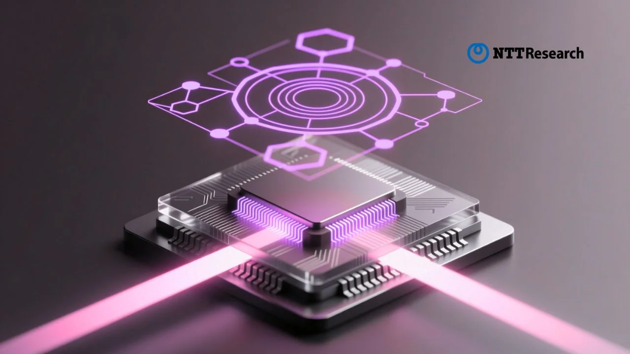
A new collaborative study has demonstrated an unprecedented level of control over light within a photonic chip, paving the way for more efficient and versatile optical computing systems. Published in the journal Nature Physics, the research details a novel, two-dimensional waveguide crafted from lithium niobate that can be dynamically reprogrammed to perform complex linear optical transformations, including machine learning inference tasks.
The work was led by scientists from NTT Research’s Physics & Informatics (PHI) Lab in collaboration with Cornell University and Stanford University. At its core, the device replaces the intricate, fixed architecture of conventional photonic integrated circuits with a single, uniformly fabricated slab that becomes functional only when illuminated with specific light patterns. This approach grants the chip approximately 10,000 programmable spatial degrees of freedom—a significant leap in reconfigurability.
The innovation addresses a fundamental constraint in integrated photonics. Traditional large-scale photonic devices are constructed from many discrete, physically defined components such as phase shifters and couplers. These elements must be individually wired, controlled, and isolated from one another, leading to significant overhead in chip area, complexity, and power dedicated to control systems.
The device developed by the NTT, Cornell, and Stanford team overturns this paradigm. In its fabricated state, the lithium niobate waveguide is a uniform, passive component. Its functionality is imparted entirely through external programming. By projecting controlled patterns of light onto the chip, researchers can locally alter the material’s refractive index—the property that governs the speed of light within a medium.
“In essence, we can paint any optical circuitry we want and then redraw it in the blink of a second,” said Martin Stein, a postdoctoral fellow at NTT Research and a lead author on the paper. This capability functions as a form of virtual wiring, where bright regions of the light pattern act as electrodes, inducing an electro-optic response in the lithium niobate without any physical electrical connections.
A key to this programmability is the integration of a distinctive silicon nitride photoconductor layer atop the lithium niobate waveguide. This layer facilitates the efficient conversion of the projected light patterns into the localized electric fields needed to tune the refractive index. This hybrid material approach combines lithium niobate’s strong electro-optic properties with practical programmability.
To validate the chip’s computational potential, the researchers tasked it with performing all-optical neural network inference. They trained the system by optimizing the refractive-index distribution—and thus the path of light waves through the chip—to solve specific problems.
A critical enabler was the development of a highly accurate physics-based model of the chip’s complex behavior, refined with empirical data. This model allowed the team to use a backpropagation algorithm to determine the exact illumination pattern needed to configure the chip for a given task.
In tests, the programmable waveguide processed data in a single optical pass, with no trainable electronic pre- or post-processing. It achieved 96% accuracy in classifying vowel sounds and 86% accuracy in recognizing handwritten digits from the standard MNIST dataset, using up to 49-dimensional input vectors. This represents a tripling of the input dimension count compared to prior comparable optical devices, showcasing the richer functionality afforded by its thousands of degrees of freedom.
The research arrives as the photonics industry seeks solutions to scalability, cost, and energy challenges. Photonic integrated circuits, which use light to perform computations like matrix-vector multiplications, are seen as a promising route to reducing the enormous energy costs associated with large-scale electronic deep learning models.
The post-fabrication programmability of this technology offers several potential industrial benefits. First, a single, general-purpose programmable chip could replace numerous application-specific photonic devices, drastically reducing research, development, and production costs. Second, the ability to reprogram a device means manufacturing imperfections can be corrected after production, which could dramatically improve wafer-scale yield—a persistent hurdle in photonics.
The paper notes that two-dimensional programmable waveguides like this one offer not just a constant-factor reduction in device area, but a superior scaling law. The required chip area grows with the number of modes at a rate of N^1.5, compared to N^2 for traditional designs. This leads to greater spatial efficiency as systems scale.
However, the authors acknowledge that the quest for energy efficiency is ongoing. While a step forward, controlling 49 modes is still far from the hundreds or thousands needed for optical computing to rival digital electronics in practical, large-scale applications. “If optical computing wants to seriously compete with digital electronic computing, we will need devices that can control hundreds or even thousands of optical modes,” Stein noted.
Beyond near-term applications in optical signal routing or sensor pre-processing, this research advances a broader vision for programmable photonics. The PHI Lab explores optics as a bridge between information science and neuroscience, and this configurable platform may enable novel studies of complex wave physics and advanced photonic phenomena.
The concept points toward a future of reconfigurable on-chip platforms that can emulate almost any functionality found in free-space optical systems. By transforming a static component into a dynamic and highly programmable canvas for light, this work marks a significant stride toward more adaptive, efficient, and powerful photonic technologies for computation, communications, and beyond.
About NTT Research
NTT Research opened its offices in July 2019 in Silicon Valley to conduct basic research and advance technologies as a foundational model for developing high-impact innovation across NTT Group’s global business. Currently, four groups are housed at NTT Research facilities in Sunnyvale: the Physics and Informatics (PHI) Lab, the Cryptography and Information Security (CIS) Lab, the Medical and Health Informatics (MEI) Lab, and the Physics of Artificial Intelligence (PAI) Group. The organization aims to advance science in four areas: 1) quantum information, neuroscience and photonics; 2) cryptographic and information security; 3) medical and health informatics; and 4) artificial intelligence. NTT Research is part of NTT, a global technology and business solutions provider with an annual R&D investment of thirty percent of its profits.