

How YES is Spearheading Semiconductor Manufacturing in India with Cutting-Edge Innovation
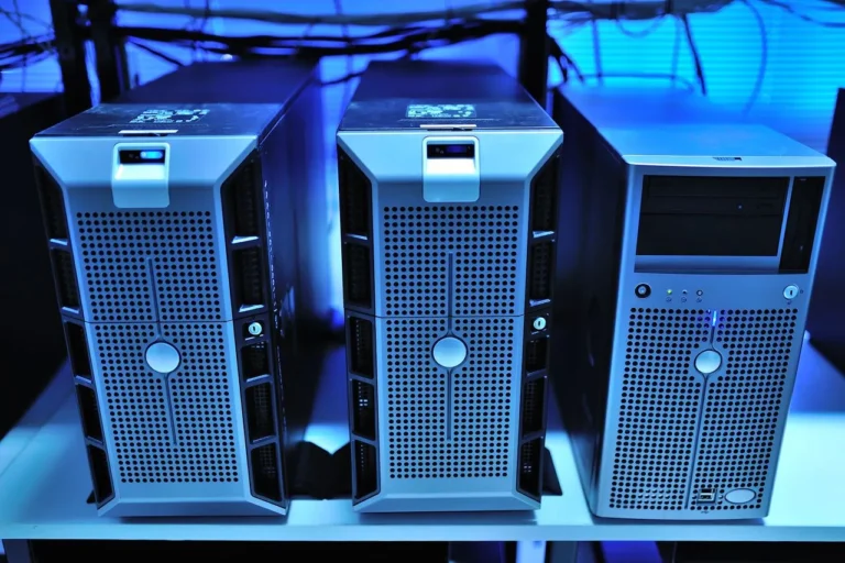
In a landmark achievement for India’s semiconductor industry, Yield Engineering Systems, Inc. (YES), a globally recognized leader in materials solutions and equipment for interfacial engineering, has successfully delivered its first commercial VeroTherm formic acid reflow tool from its state-of-the-art manufacturing facility in Sulur, Coimbatore. This milestone marks a pivotal moment not only for YES but also for India’s burgeoning semiconductor ecosystem, as it represents the country’s first locally manufactured equipment designed for advanced semiconductor applications such as High Bandwidth Memory (HBM)—a critical component for artificial intelligence (AI) and high-performance computing (HPC) technologies.
YES officially launched operations at its new Sulur facility in September 2024. Located at 96/3 Vadakku Sambala Thottam, Trichy Road, Kannampalayam, Sulur Taluk, this cutting-edge facility is a cornerstone of YES’s global expansion strategy. The facility is designed to enhance operational efficiency for YES’s customers worldwide while supporting India’s growing demand for advanced semiconductor manufacturing capabilities.
With over four decades of expertise in developing equipment for the semiconductor, display, and life sciences industries, YES has earned a reputation for innovation and reliability. The Sulur facility is equipped with state-of-the-art technology to produce advanced systems like the VertaCure™, Verotherm™, and VeroFlex™, which are essential for wafer and panel-level packaging applications. By establishing this facility, YES aims to build a robust local supply chain, create employment opportunities, and contribute to India’s vision of becoming a global semiconductor hub.
The delivery of the first VeroTherm tool underscores YES’s commitment to advancing India’s semiconductor manufacturing capabilities. S. Krishnan, Secretary, Ministry of Commerce and Industry, praised the initiative, stating, “The commencement of shipments from the YES manufacturing facility in Tamil Nadu represents a remarkable step forward for the Indian semiconductor industry. This aligns perfectly with our national vision of building a self-reliant and robust semiconductor ecosystem. We are committed to providing all necessary support to foster further growth and innovation in this sector, thereby strengthening India’s position in the global semiconductor market.”
The achievement also reflects the success of Tamil Nadu’s proactive policies aimed at fostering semiconductor development. T. R. B. Rajaa, Tamil Nadu Industries Minister, highlighted the state government’s efforts, saying, “This milestone is yet another achievement stemming from Honorable Chief Minister Thiru M. K. Stalin’s US tour last year and the Tamil Nadu Semiconductor and Advanced Electronics Policy. Despite global and national challenges, Tamil Nadu remains steadfast in its mission to become a global semiconductor hub. In the TN Budget 2025, we announced semiconductor manufacturing parks in Sulur and Palladam under a new Rs 500 billion Semiconductor Mission.”
For YES, the Sulur facility is more than just a manufacturing hub—it’s a fully integrated part of the company’s global network. Ramakanth Alapati, Chairman and CEO of YES, emphasized this point, stating, “This milestone underscores our unwavering commitment to strengthening the Indian semiconductor ecosystem, enabling the efficient delivery of our products to customers in India and beyond. This facility ensures that we consistently provide our customers with the reliability and technical expertise they expect.”
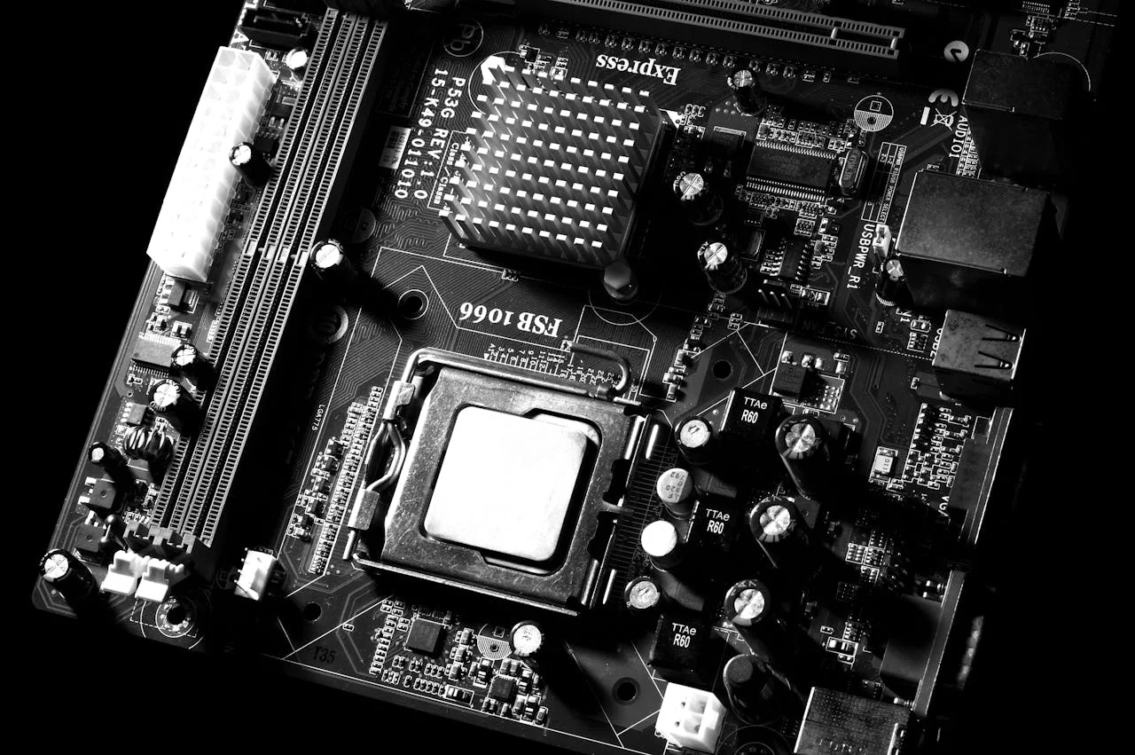
By leveraging its decades of experience and cutting-edge technology, YES is well-positioned to meet the demands of next-generation semiconductor applications. The company’s product portfolio includes vacuum curing, coating, annealing, fluxless reflow, via plating, cavity etching, and electroless deposition tools—essential for producing advanced packaging solutions for wafers and glass panels. These innovations are critical for driving advancements in AI, HPC, memory systems, and life sciences.
The establishment of YES’s Sulur facility is expected to have a transformative impact on the local economy. By creating jobs and fostering collaboration with local suppliers, the facility will play a crucial role in building a sustainable semiconductor ecosystem in India. Moreover, YES’s investment aligns with the Indian government’s Atmanirbhar Bharat (Self-Reliant India) initiative, which seeks to reduce dependency on imports and establish India as a global manufacturing powerhouse.
As global demand for semiconductors continues to rise, YES’s expansion into India positions the company—and the country—at the forefront of this rapidly evolving industry. The successful delivery of the first VeroTherm tool is just the beginning. With plans to scale production and introduce additional advanced technologies, YES is poised to play a key role in shaping the future of semiconductor manufacturing in India.
For more information about YES and its groundbreaking contributions to the semiconductor industry, visit YES.tech.