Avicena Unveils Breakthrough in Ultra-Low Power microLED Interconnects at ECOC 2025
In a groundbreaking development, Avicena, the trailblazer in next-generation microLED interconnects, has announced a significant milestone at ECOC 2025. The company showcased a fully operational microLED-based optical link with an industry-leading transmitter (Tx) power consumption of just 200 femtojoules per bit (fJ/bit). This achievement underscores the remarkable efficiency of Avicena’s scalable LightBundle™ platform, designed to meet the demands of high-performance computing (HPC) and artificial intelligence (AI) data centers. By leveraging a high-sensitivity receiver adapted from a high-volume foundry camera sensor process, the demonstration achieves dramatically reduced microLED drive currents, setting a new benchmark for energy-efficient optical communication.
Revolutionizing Optical Links with microLED Technology
The live demonstration at ECOC 2025 highlights Avicena’s ability to operate its microLED-based optical links at incredibly low power levels while maintaining exceptional performance. Running at a raw bit error rate (BER) of less than 1E-12—without the need for forward error correction—the system operates at a drive current of approximately 0.25mA and a data rate of 4Gb/s. The microLED is paired with a hybrid-bonded camera sensor and a discrete transimpedance amplifier (TIA), showcasing the potential of this innovative approach.
Unlike traditional laser-based systems that require threshold currents to function, microLEDs can operate efficiently even at very low drive currents. This unique characteristic allows them to deliver high-speed data transmission without compromising energy efficiency. The result is a transformative solution that eliminates many of the limitations associated with legacy optical interconnects.
The Scalable LightBundle™ Platform: Redefining Connectivity
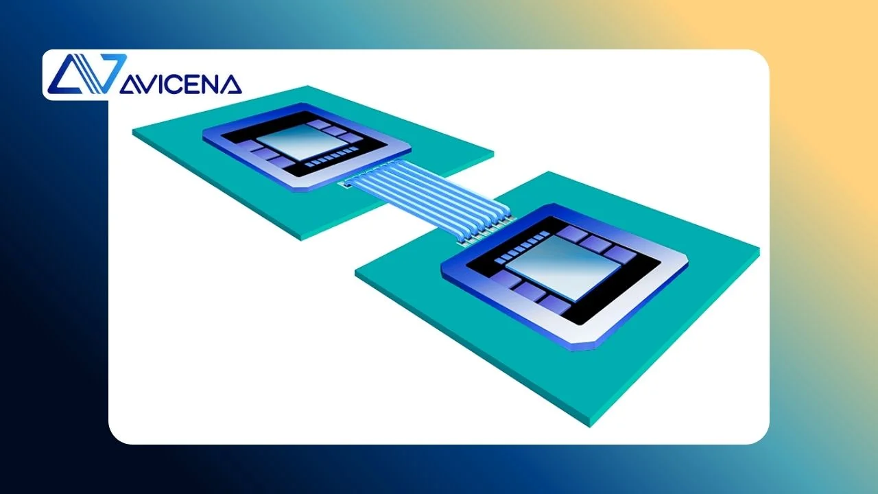
At the heart of Avicena’s innovation is its LightBundle chiplet platform, which is redefining how data is transmitted within advanced computing architectures. Traditional optical interconnects serialize low-speed on-chip data into very high-speed optical lanes, adding complexity and latency to the system. In contrast, LightBundle transmits raw parallel data directly, simplifying the architecture and enabling massive arrays of microLEDs to achieve unprecedented aggregate bandwidth.
This approach delivers several key advantages:
- Low Latency: By eliminating the need for serialization, LightBundle reduces the time required to process and transmit data.
- Low Power Consumption: Operating at 200fJ/bit, the platform sets a new standard for energy efficiency in optical interconnects.
- Ease of Integration: LightBundle chiplets are compatible with any silicon node, making them highly versatile for various packaging architectures, including co-packaged optics (CPO), on-board optics (OBO), pluggable optical modules, and wide memory interconnects.
These features make LightBundle an ideal solution for addressing the growing demands of AI and HPC platforms, where bandwidth, latency, and power consumption are critical factors.
A Leap Forward for GPU-to-GPU and Memory Interfaces
While the implications of this breakthrough extend far beyond GPU-to-GPU connectivity, one of the most exciting applications lies in High Bandwidth Memory (HBM) interfaces. These interfaces represent the next frontier for optical interconnects, requiring wide buses with minimal latency to overcome traditional memory bandwidth bottlenecks. LightBundle’s ability to transmit low-speed parallel data at ultra-low power and latency positions it as a game-changing technology for breaking these barriers.
“By leveraging a highly sensitive receiver, a minor modification to a high-volume camera process, and the unique properties of microLEDs, we can achieve unmatched energy efficiency in our LightBundle interconnects,” said Bardia Pezeshki, CTO of Avicena. “This breakthrough shows how microLED technology can replace legacy laser-based links with a simpler, more scalable, and far lower power solution.”
Marco Chisari, CEO of Avicena, echoed this sentiment, emphasizing the broader impact of the innovation. “The implications of this innovation extend beyond GPU-to-GPU connectivity,” he said. “HBM memory interfaces are one of the next great frontiers for optical interconnects and ideally require wide buses with minimal latency. LightBundle’s ability to directly transmit low-speed parallel data at very low power and low latency makes it ideally suited to breaking traditional memory bandwidth bottlenecks, and opening the door to new system architectures for next-generation AI and HPC platforms.”
Scaling AI Clusters with Energy Efficiency
This demonstration builds on Avicena’s ongoing collaborations with hyperscale data center partners to enable scale-up GPU clusters spanning multiple racks and thousands of GPUs. By integrating LightBundle into these environments, Avicena aims to dramatically scale AI clusters while reducing their overall power consumption. The platform’s unparalleled energy efficiency not only addresses the pressing need for sustainable computing solutions but also paves the way for new system architectures that can support the exponential growth of AI workloads.
A Vision for the Future of Optical Interconnects
Avicena’s latest achievement marks a pivotal moment in the evolution of optical interconnects. By combining microLED technology with optimized camera sensors, the company has created a solution that is both highly efficient and scalable. This innovation has the potential to transform not only AI and HPC platforms but also other areas such as telecommunications, autonomous vehicles, and consumer electronics.
As the demand for faster, more energy-efficient data transmission continues to grow, technologies like LightBundle will play a crucial role in shaping the future of connectivity. Avicena’s work demonstrates that the path to next-generation computing lies in embracing simplicity, scalability, and sustainability—a vision that promises to unlock new possibilities across industries.
About Avicena
Avicena Tech Corp. is a privately held company located in Sunnyvale, CA, developing LightBundle, a next generation optical interconnect architecture for AI/ML, HPC, sensors, 5G wireless and aerospace applications. This unique, flexible ultra-low energy technology is based on microLEDs, offering both very high bandwidth and low latency. Now, system designers can disaggregate functions like compute and memory and radically grow system throughput. Avicena’s technology is a key building block in the evolution of networking and computing that will reduce the energy impact on our planet.


