


The rise of AI PCs and edge AI applications has accelerated demand for high-performance, power-efficient interfaces in system-on-chips (SoCs). Since entering the market in 2023, AI PCs have seen rapid adoption. Analysts at Gartner forecast shipments of 77 million units in 2025, accounting for 31% of the global PC market, with that figure climbing to 55% in 2026. Edge AI growth stems from compact algorithms, advanced AI processors, and the expanding IoT ecosystem.
Modern devices like laptops, AI PCs, and high-end imaging hardware push SoCs to deliver greater bandwidth at ultra-low voltages while minimizing electromagnetic interference (EMI) and radio-frequency interference (RFI). Processes at 5nm and finer nodes must juggle these constraints amid rising needs from high-resolution sensors, elevated frame rates, and AI processing loads.
Cadence has introduced an eUSB2V2 intellectual property (IP) solution tailored to these demands. Fabricated on a 3nm node and aligned with the eUSB2V2 specification, it achieves data rates up to 4.8 Gbps using low I/O voltages. This setup ensures strong signal integrity, adaptable data rates, and reduced power draw, suiting next-generation SoCs.
Cadence marked a key achievement earlier this year with the tapeout and full silicon validation of its inaugural 3nm eUSB2V2 physical layer (PHY) test chip. Expanding on this foundation, the company has now assembled a comprehensive eUSB2V2 ecosystem, encompassing host and device controller IP alongside the PHYs.
At CES 2026, Cadence plans to present a live, end-to-end eUSB2V2 demonstration—the first of its kind. This setup integrates host and device PHYs with controllers, showcasing operational performance in a practical configuration. Such a display highlights potential applications in AI PCs and edge AI platforms, signaling readiness for broader deployment.
The controllers stand alone as drop-in replacements for older USB 2.0 or eUSB2v1 implementations, optimizing power, performance, and area (PPA). They integrate smoothly with USB 3.2 or USB 2.0 stacks, easing subsystem upgrades with low risk. Compliance with UTMI 2.0 enables symmetric or asymmetric rates up to 4.8 Gbps, including high-speed native operations.
Cadence designed these controllers to simplify eUSB2V2 adoption in SoCs for PCs and consumer electronics. They incorporate targeted enhancements for efficiency and versatility.
The architecture pairs eUSB2V2 controllers with USB 3.x and USB 2.0 (eUSB2v1) elements. Designers can add eUSB2V2 ports to multi-port setups or swap out individual USB 2.0 interfaces. Configurations range from standalone deployments to hybrid systems blending eUSB2V2 with USB 3.x and USB 2.0.
This modularity allows attachment to existing USB 3.x designs without alterations, minimizing disruption. Cadence complements the hardware with a full suite: PHYs, controllers, software drivers, Linux references, and verification IP (VIP).
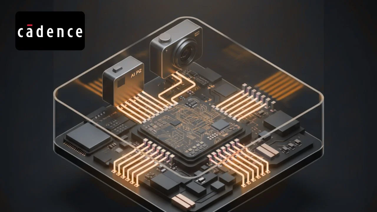
Live demonstrations carry significant weight in validating high-speed links. Cadence’s CES setup employs 3nm eUSB2V2 PHY test chips for host and device roles, with controllers on field-programmable gate array (FPGA) boards.
A high-resolution camera feeds maximum raw data in real time via PC/ATX boards to the FPGA. The host FPGA connects to a PC/ATX system and display, rendering the video stream. This chain—from capture to output—demonstrates eUSB2V2’s capability in handling intensive, real-world data flows.
Rigorous testing underpins the solution’s claims. Cadence engineers conducted far-end eye diagram analysis at 18.5 dB inter-symbol interference (ISI), yielding clear results at 4.8 Gbps. These metrics confirm error-free transmission, low jitter, and resilience across conditions.
Such validation is critical for SoC designers relying on IP for production silicon. It proves the link’s stability in noisy environments typical of densely packed edge devices.
This end-to-end eUSB2V2 showcase represents a pivotal step in interface evolution. It combines host and device components into a working prototype, addressing speed, power, and interference challenges head-on.
eUSB2V2 slots into Cadence’s extensive interface portfolio, which covers USB 3.x, MIPI, DisplayPort, embedded DisplayPort, and PCIe. This breadth supports cohesive designs for edge AI consumer applications, from enhanced imaging to responsive AI processing.
For SoC teams, the demo offers tangible evidence of integration feasibility. It lowers barriers to adopting advanced nodes, fostering architectures that balance performance with efficiency. As AI PCs and edge systems proliferate, reliable interfaces like eUSB2V2 will underpin scalable innovations.
In the competitive landscape of AI hardware, validated IP solutions accelerate time-to-market. Cadence’s approach—spanning silicon-proven PHYs to software stacks—equips developers to meet escalating bandwidth demands without compromising on power budgets or signal quality.