
Optimizing the Nano-TSV-to-BPR Connection in Backside Power Networks
As technology nodes continue to scale, maintaining power and performance while reducing the footprint has become increasingly challenging. Backside power delivery networks (BSPDNs) address this challenge by moving the power delivery network to the wafer backside.
- Using SEMulator3D®, engineers can create a realistic virtual model of the connection between nano-TSVs (nTSVs) and buried power rails
- A study was conducted on the impact of nTSV overlay and patterning effects
- The results showed that rounded corners increase sensitivity to overlay-induced resistance
What Is Backside Power Delivery (BSPDN)?
The problem being solved by BSPDNs is similar to getting people out of a crowded office. If everyone uses the same front hallway, it gets packed and slows people down. But if you add a second hallway in the back just for deliveries, the front hallway is less crowded, and everything moves more smoothly. In the same way, backside power delivery sends power through the “back hallway,” leaving the front side of the chip less congested.
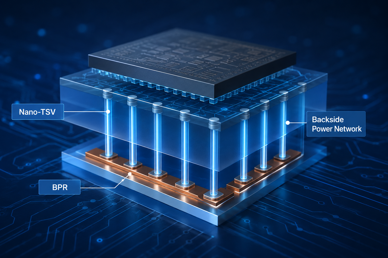
To enable BSPDNs, nano-through-silicon vias (nTSVs) are connected to buried power rails (BPRs), which move some of the power wiring lower into the chip. This relieves frontside routing congestion and improves signal integrity.
Key Process Challenges: Overlay and Patterning Effects
While effective, this design introduces critical process challenges:
- Overlay variation during nTSV alignment
- Corner rounding during patterning
These factors directly impact nTSV-BPR connection resistance and thus chip performance and yield.
The Semiverse® Solutions team, in conjunction with our colleagues at imec, recently analyzed BSPDN technology processes and performance using a predictive simulation in SEMulator3D®. We evaluated the impact of nTSV overlay and patterning effects on nTSV resistance to identify possible margins for process optimization.
Modeling nTSV Resistance Using SEMulator3D
A SEMulator3D virtual measurement was used to perform resistance extraction of a cross-bridge Kelvin resistor (CBKR) structure to optimize the nTSV-BPR connection, since the CBKR isolates the resistance of the connection from the contribution of the metal lines (Figure 1). The left drawing displays the TSV line resistance, which measures the resistance of the complete electrical path that passes through the TSV, including the copper conductor inside the TSV and any top and bottom TSV connections. The drawing on the right displays the TSV Kelvin resistance, which isolates out the resistance of the metal lines. Only the resistance of the TSV connections is measured in the right-hand diagram.
Using SEMulator3D virtual fabrication, a full process step sequence was simulated to reproduce realistic process effects in the model of a full CBKR structure.
Figure 2 displays an nTSV-BPR TEM cross-section along with the matching process simulation result. The simulation accurately reproduced the resulting nTSV-BPR profile and shape.
To move beyond idealized cylindrical or polygonal vias, the full process flow was simulated in SEMulator3D so that realistic profile details could be captured. The modeled CBKR structure reproduced the observed nTSV-BPR cross-section, enabling resistance extraction on process-realistic geometries and improving the relevance of comparisons with electrical measurements.
In our study, we simulated both TSV patterning corner-rounding effects and TSV overlay effects.
Figure 3 depicts two nTSV patterning configurations simulated using SEMulator3D: one without corner rounding and one with corner rounding.
Simulation Highlights: Key Findings
The results showed that rounded corners increase sensitivity to overlay-induced resistance, making realistic patterning effects essential for accurate modeling.
Simulation results demonstrated that the nTSV overlay needs to be less than 30 nm to guarantee a safe connection between the nTSV and the BPR. The nTSV-BPR connection is more sensitive to overlay problems when using rounded corners compared to when using a square section. Thus, TSV patterning rounding effects are critical and need to be considered in any resistance simulation.
The process simulation using realistic profiles was then coupled to a virtual electrical simulation to provide a predictive nTSV-BPR resistance model. A process variability evaluation of low nTSV resistance was then performed. BPR contact area optimization and the impact of nTSV overlay variation on nTSV-BPR chain link resistance was also explored.
Figure 5 displays the impact of the nTSV overlay on resistance using an nTSV with patterning rounding.
Simulated resistance was also benchmarked against actual nTSV resistance measurements. Our simulations reproduced the minimum values of the measurement distribution, validating the simulated resistance model. Simulations indicated that resistance reduction and tighter control were achieved when the nTSV overlay was limited to about 15 nm.