


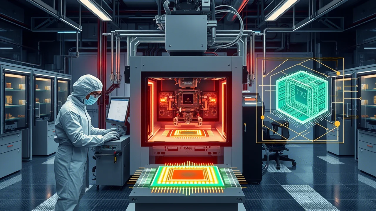
In a groundbreaking move to address the semiconductor industry’s toughest scaling challenges, Lam Research Corp. (Nasdaq: LRCX) has introduced Akara®, the most advanced conductor etch tool available today. This revolutionary innovation in plasma etch technology delivers unmatched precision and performance, enabling chipmakers to create atomic-scale features required for next-generation 3D devices. With its proprietary technologies and cutting-edge capabilities, Akara represents a generational leap forward in conductor etch solutions, empowering the semiconductor industry to meet the demands of increasingly complex architectures.
Akara builds on Lam Research’s legacy of over two decades of continuous innovation in conductor etch technology. Leveraging the company’s proprietary DirectDrive® technology, Akara achieves plasma responsiveness that is 100x faster than previous generations, delivering unparalleled control and precision at the atomic level.
“Building on more than 20 years of continuous conductor etch innovation, our groundbreaking new Akara etcher leverages Lam’s proprietary DirectDrive® technology to deliver the controlled creation of atomic-scale features with plasma responses that are 100x faster,” said Sesha Varadarajan, Senior Vice President of the Global Products Group at Lam Research. “Akara is a generational leap forward in conductor etch capabilities for shaping small, complex structures for the 3D era of chips.”
This advancement extends Lam’s leadership in conductor etch technology, which includes multiple generations of the highly successful Kiyo® conductor etch tool. Introduced in 2004, Kiyo® has been deployed in over 30,000 chambers worldwide, cementing Lam’s reputation as a pioneer in plasma etch solutions.
As the semiconductor industry transitions to more advanced architectures, such as gate-all-around (GAA) transistors, 6F2 DRAM, and 3D NAND devices, the demand for precise and reliable etch solutions has never been greater. These cutting-edge devices require angstrom-level precision to create small features with progressively higher aspect ratios—capabilities that exceed the limits of mainstream plasma etch technologies.
Akara addresses these challenges with its suite of proprietary innovations:
These advancements make Akara indispensable for scaling advanced architectures, including 4F2 DRAM, complementary field-effect transistors (CFETs), and 3D DRAM.
Designed for high-volume manufacturing, Akara maximizes process yield while maintaining millisecond response times. Its sophisticated etch uniformity controls ensure wafer-to-wafer repeatability, a critical factor for achieving consistent performance in mass production. Integrated on Lam’s high-productivity Sense.i® platform, Akara also leverages Equipment Intelligence® solutions for automated maintenance, reducing equipment upkeep and enhancing operational efficiency.
“Akara is not just a technological breakthrough—it’s a solution optimized for the realities of modern semiconductor manufacturing,” said Varadarajan. “Its ability to deliver precision at scale ensures that chipmakers can meet the growing global demand for semiconductors while driving down costs and improving yields.”
Akara has already been selected as the production tool of record by leading device manufacturers for advanced planar DRAM and foundry GAA applications. Its value has been validated through repeat orders and a rapidly growing installed base, underscoring its critical role in enabling next-generation semiconductor architectures.
“As global demand for semiconductors continues to grow, innovative technology solutions from our partners are required to enable new, more powerful device architectures,” said Dr. Y.J. Mii, Executive Vice President and Co-Chief Operating Officer at TSMC. “Critical plasma etch capabilities will be an integral part of solving the many production challenges these new devices pose.”
The introduction of Akara coincides with the announcement of ALTUS® Halo, the world’s first molybdenum atomic layer deposition (ALD) tool in production. Together, these innovations highlight Lam Research’s commitment to delivering the technologies needed to address upcoming semiconductor inflections. By providing comprehensive solutions for both etch and deposition processes, Lam is equipping chipmakers with the tools they need to stay ahead in an increasingly competitive market.
The semiconductor industry is at a pivotal moment, with demand for advanced chips surging across industries such as AI, automotive, and consumer electronics. As device architectures become more complex, the need for precise, scalable, and efficient manufacturing solutions has never been more critical. Akara’s ability to deliver atomic-scale precision and unmatched performance positions it as a cornerstone of next-generation semiconductor production.
By addressing the challenges of gate-all-around transistors, 3D NAND, and DRAM scaling, Akara ensures that chipmakers can continue to push the boundaries of innovation. Its integration into high-volume production lines demonstrates Lam Research’s dedication to delivering practical, scalable solutions that drive the industry forward.