

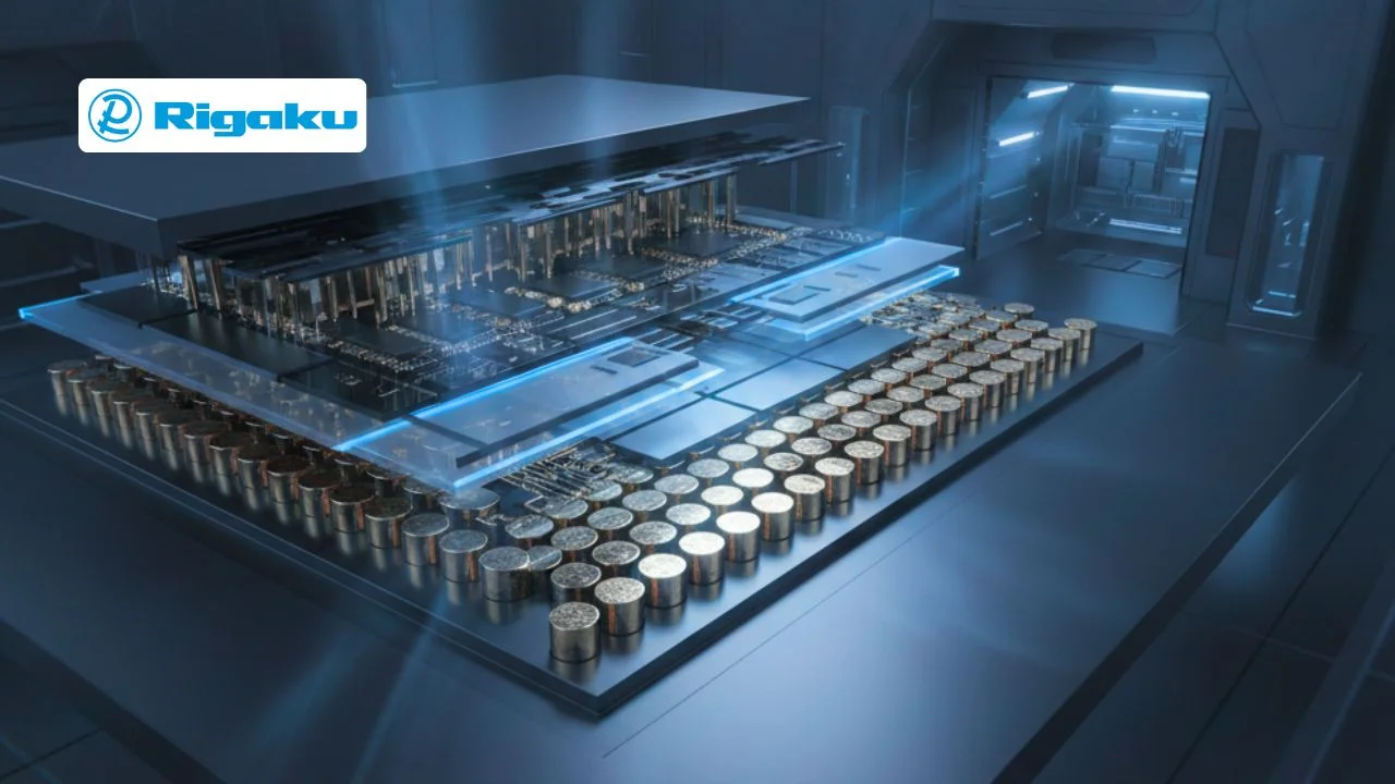
Rigaku Corporation, a Tokyo-based provider of X-ray analytical instruments and part of Rigaku Holdings, has unveiled the ONYX 3200, a specialized metrology system designed for semiconductor manufacturing. This tool targets critical measurements in wafer-level processes, including film thickness, material composition, and microscopic bump structures. Engineers developed it to support quality control and yield improvement specifically in back-end-of-line (BEOL) metal wiring and advanced packaging stages.
Semiconductor production faces mounting pressures from sectors like artificial intelligence, high-performance computing, and data centers. These demands push chip designs toward finer interconnects and more intricate packaging. Metal layers, often thinner than a human hair, and bumps smaller than 10 micrometers demand precise, non-destructive inspection to ensure device reliability and performance.
The ONYX 3200 addresses these challenges by consolidating measurements that traditionally required separate systems. It performs comprehensive inspections of metal features—from wiring layers to interconnect bumps—on a unified platform, streamlining workflows in high-volume fabs.
Modern chips integrate billions of transistors, connected through dense networks of metal lines and vias in the BEOL phase. As nodes shrink below 3nm, these structures become more susceptible to variations in thickness, composition, and geometry. Packaging adds further complexity, with hybrid bonding and 3D stacking relying on precise bump placement for electrical and mechanical integrity.
Non-destructive metrology proves essential here. Destructive cross-sectioning wastes wafers and slows feedback loops, while optical methods struggle with opaque metals. X-ray fluorescence (XRF) excels at composition but lacks height profiling. The ONYX 3200 bridges these gaps, enabling fabs to monitor process stability without compromising throughput.
Industry analysts note that yield losses from BEOL defects can exceed 20% in advanced nodes. Tools like the ONYX 3200 help mitigate this by providing data for real-time adjustments, aligning with broader trends in digital transformation for semiconductor supply chains.
The system’s design centers on handling multi-layer metal stacks and solder bumps, common in flip-chip and advanced packaging. It combines optical and X-ray techniques for a holistic view.
Bumps typically feature a lower conductive layer—often copper or nickel—capped by a tin-silver (SnAg) alloy for soldering. Traditional optical confocal microscopy absorbs signals in the upper layer, obscuring lower dimensions. The ONYX 3200 employs a high-resolution 3D confocal scanner to map overall bump topography and height.
Paired with this is a fluorescent X-ray detector that quantifies upper-layer thickness and composition. By subtracting X-ray-derived values from the optical total height, the system isolates lower-layer metrics with sub-micrometer precision. This method establishes reliable baselines for interconnect strength, critical as bump pitches drop below 20 micrometers in next-generation packages.
Rigaku engineered a proprietary dual-head X-ray source to tackle composition analysis. One head focuses on low-concentration elements, detecting silver in SnAg bumps down to 2% with a precision of 0.04% (4 parts per 100,000). This level of accuracy supports tight control over alloy ratios, which directly affect joint reliability under thermal cycling.
The second head handles broader surveys of surrounding metal features, such as copper redistribution layers or barrier films. Simultaneous operation boosts measurement speed, allowing scans of full 300mm wafers in minutes rather than hours. This flexibility suits diverse processes, from high-bandwidth memory (HBM) stacking to chiplet integration.
Beyond core sensing, the ONYX 3200 incorporates automation features for fab environments. It supports automated wafer handling, compatible with FOUP carriers, and integrates with standard SECS/GEM protocols for factory data exchange. Software provides real-time analytics, overlaying 3D models with composition heatmaps for defect root-cause analysis.
Resolution specs include:
Users report setup times under 30 minutes per recipe, with minimal recalibration between lots. Energy-efficient operation and a compact footprint (under 2m²) make it viable for cleanroom integration alongside tools like CVD or electroplating stations.
This launch aligns with surging investments in advanced packaging. TSMC, Intel, and Samsung have ramped up capacity for CoWoS, Foveros, and I-Cube technologies, where metrology bottlenecks limit scaling. Rigaku positions the ONYX 3200 as a response to these needs, building on its established X-ray portfolio used by major foundries.
One early deployment has occurred at a leading global foundry’s advanced packaging line, validating performance in production. Rigaku anticipates sales of ¥1.5 billion in fiscal 2026, scaling to ¥3 billion by 2027 as BEOL adoption grows. This trajectory reflects broader market growth; SEMI projects semiconductor metrology spending to rise 12% annually through 2030, driven by AI chip demand.
Competitors like KLA and Applied Materials offer similar systems, but Rigaku emphasizes the ONYX 3200’s single-platform efficiency. Independent benchmarks will determine its edge in total cost of ownership, though initial feedback highlights throughput gains of 2-3x over legacy multi-tool setups.
Adopting tools like the ONYX 3200 could reshape quality assurance in semiconductors. Fabs gain granularity to correlate metrology data with electrical test results, accelerating process ramps. For instance, precise SnAg control reduces voiding in solder joints, a common failure mode in high-density interconnects.
As 2.5D/3D architectures proliferate, such systems support heterogeneous integration—combining logic, memory, and photonics on single packages. This capability underpins next-gen AI accelerators, where interconnect density rivals transistor scaling.
Challenges remain, including calibration for emerging materials like cobalt or ruthenium barriers. Rigaku signals ongoing R&D to extend the platform, potentially incorporating AI-driven anomaly detection.
About the Rigaku Group
Since its establishment in 1951, the engineering professionals of the Rigaku group have been dedicated to benefiting society with leading-edge technologies, notably including its core fields of X-ray and thermal analysis. With a market presence in 136 countries and regions and some 2,000 employees from 9 global operations, Rigaku is a solution partner in industry and research analysis institutes. Our overseas sales ratio has reached approximately 70% while sustaining an exceptionally high market share in Japan. Together with our customers, we continue to develop and grow. As applications expand from semiconductors, electronic materials, batteries, environment, resources, energy, life science to other high-tech fields, Rigaku realizes innovations “To Improve Our World by Powering New Perspectives.”
For details, please visit: rigaku-holdings.com/english